
Crystals are more than just beautiful natural formations; they are essential components in the advancement of optical and electrical technologies.
When we think of crystals, we often picture dazzling gemstones or shimmering snowflakes. However, the practical applications of crystals go far beyond their aesthetic appeal. In the world of science and technology, crystals are integral in the creation of materials used in optical and electrical devices. Understanding how to control and manipulate crystal growth is crucial for enhancing the performance and efficiency of these devices.
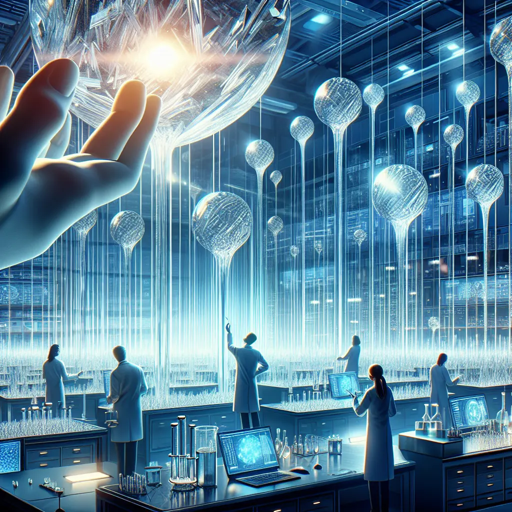
The Science Behind Crystal Growth
Crystals, such as those found in table salt and refined sugar, appear white to us due to the way their individual colorless particles scatter visible light. While this scattering can be aesthetically pleasing, it poses challenges in technological applications where clarity and precision are paramount. In optical and electrical devices, the goal is often to achieve thin films with neatly arranged crystal structures to maximize effectiveness.
Key Considerations in Crystal Formation:
Advancements in Crystal Growth Techniques
Recent advancements in crystal growth techniques have allowed scientists to better control the quality and arrangement of crystals. By refining these methods, researchers are able to produce fine thin films that meet the exacting standards required for cutting-edge technologies.
For instance, techniques such as molecular beam epitaxy and chemical vapor deposition have been pivotal in improving the precision of crystal growth. These methods enable the creation of complex crystal structures layer by layer, offering greater control over the final product's properties.
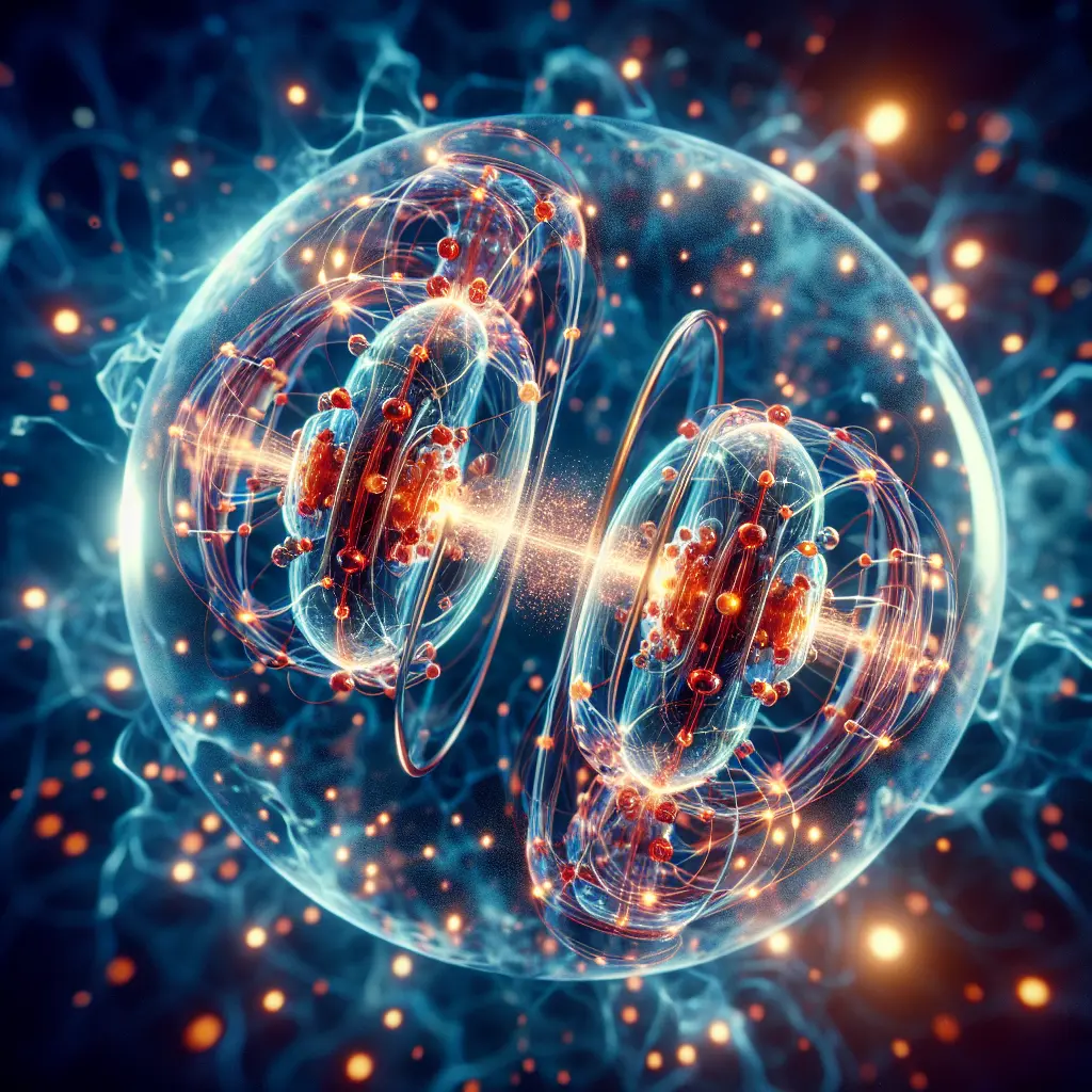
The Importance of Quality Control
Quality control in crystal growth is paramount for developing effective optical and electrical devices. With meticulous oversight and innovative techniques, scientists can produce materials that significantly enhance the capabilities of technologies such as lasers, sensors, and semiconductors.
Exploring Further
As our reliance on sophisticated technology continues to grow, the demand for high-quality crystal materials will only increase. The ongoing research in this field promises to unlock new potentials and possibilities, driving innovation forward.
To delve deeper into the intricacies of crystal growth and its implications for technology, you can explore more through this article.
As we continue to uncover the mysteries of crystals and harness their potential, it becomes evident that these natural wonders are as much about practicality as they are about beauty.
Until next time, may your days be as clear and structured as a perfectly formed crystal.


Leave a Comment